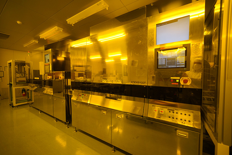
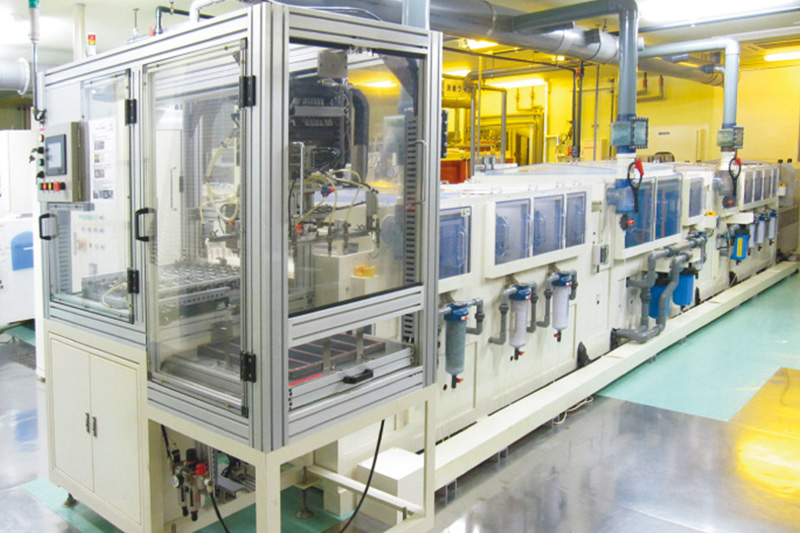
01
Drilling
Make through holes on boards at specified coordinates by turning the drill at high speed. The drills have the diameter of minimum 0.06 mm up to 4.0 mm and the highest rotation speed is 30,000 per minute.
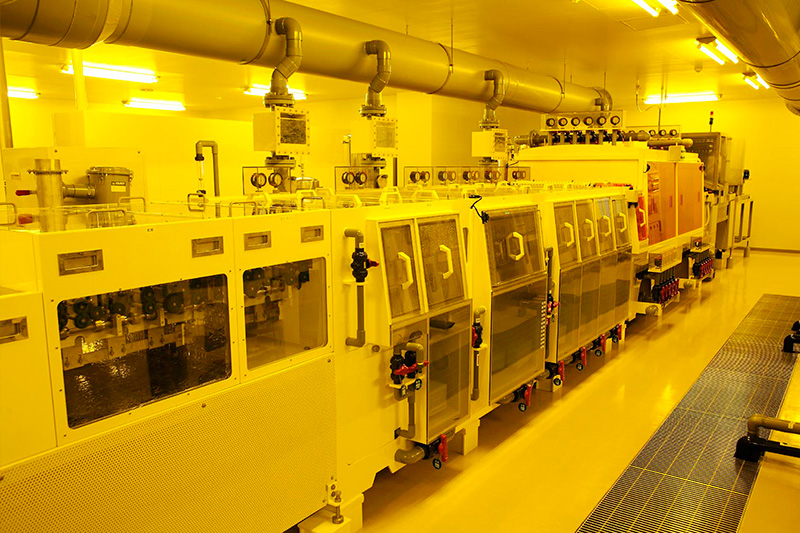
02
Copper Plating
Make copper plating on board surfaces and side surfaces of the through holes so that electrical connections between both sides of the boards are secured. The plating thicknesses vary from a minimum of 8 um up to about 30 um for different products.
03
Laminating (Circuit forming)
Compress a photosensitive film on the board surfaces for making wiring. The film thicknesses vary from a minimum of 10 um up to about 50 um for different products.
04
Pattern Exposure (Circuit forming)
Place artwork film for exposure and irradiate ultraviolet rays to the areas where wiring is made, while keeping the other areas shielded from the exposure.
05
Development (Forming circuit)
Remove the photosensitive film from the areas where no wiring is made using a specialized alkaline solvent.
06
Etching and Stripping (Circuit forming)
Melt and remove unnecessary copper to leave the intended wiring. The following reaction enables the process: FeCl3 + CuC1 -> FeCl2 + CuCl2
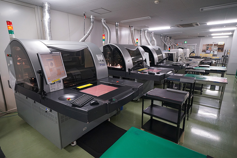
07
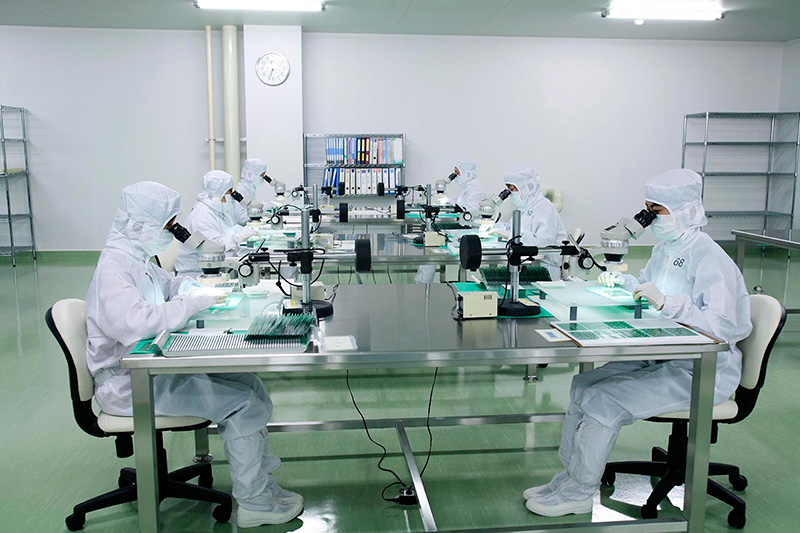
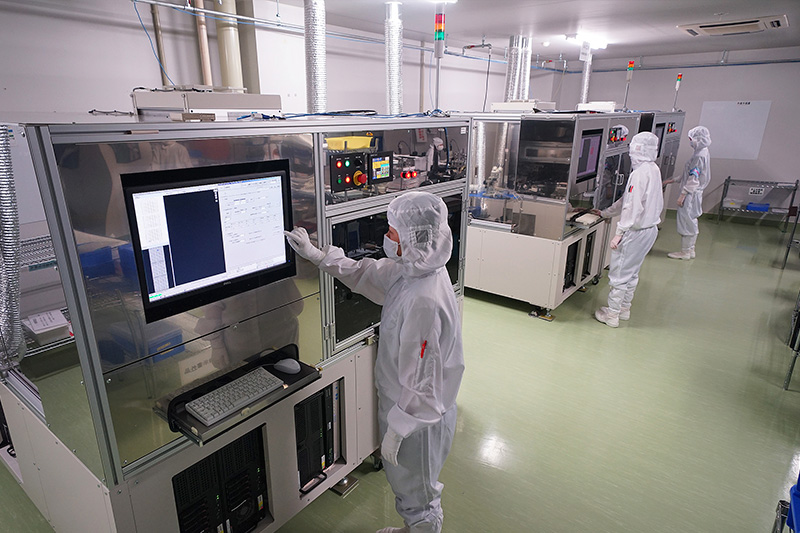
AOI (Pattern Inspection)
Inspect the formed wiring in this automatic optical inspection process for any defectiveness based on the design data.
08
Pretreatment (Liquid resist)
Roughen the copper surface of the wiring to enhance cohesiveness between the wiring and a protective coating which will be applied on the wiring.
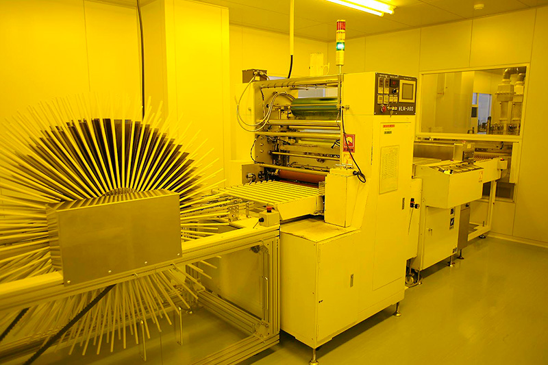
09
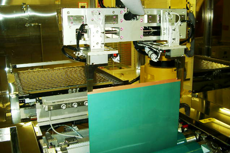
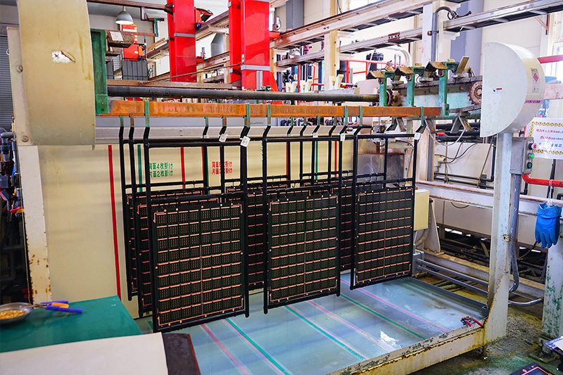
Printing (Liquid resist)
Apply photosensitive ink on the board surface to form a protective coating. Two application schemes are available in this process, roll coater and screen printing.
(Photo: Roll coater)
10
Pattern Exposure (Liquid resist)
Place artwork film for exposure and irradiate ultraviolet rays to the areas where wiring is made, while keeping the other areas shielded from the exposure.
11
Development (Liquid resist)
Melt and remove unnecessary photosensitive ink from areas where Au plating will be applied using a specialized alkaline solvent.
12
Au Plating
Make nickel or gold deposition on pads, terminals and some other areas of printed boards to make connections to IC chip.
13
Routing
Make a complete shape of printed board to specified geometry and size with an automatic router machine using a router bit.
14
Cleaning
Clean and remove any dirt off of board surfaces using a specialized solvent, pure water, and ultrasonic waves before the final inspection.
15
AFVI (Final Inspection)
Perform final automatic optical inspection to make sure that completed printed circuit boards contain no cosmetic defectiveness before being delivered to our customers.
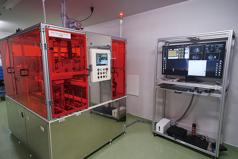
16
Laser Marking
Print 2D codes for tracking the production history and defectiveness related identifications on completed printed circuit boards using laser marking.
17
Quality Assurance Test
Perform tests and measurements on the products to assure reliability and conformity to customers required specifications before approving delivery to customers.